Home Products Support Company Links  
   

»

 Altera ACEX Development Board

EZ1KUSB - Altera ACEX FPGA Development board with USB interface

EZ1KUSB - Altera ACEX FPGA development board with USB interface

Datasheet: EZ1KUSB_Datasheet.pdf

Block Diagram: EZ1KUSB Block Diagram

Schematics: ez1kusb_sch_02.pdf

Key Features:

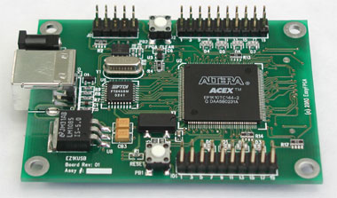
  • Connects to the host PC via USB

  • USB data transfer rate up to 1 MB/s (One MegaByte per second)

  • Easy and fast FPGA configuration via USB or JTAG

  • High Density FPGA (10,000 to 50,000 typical gates, up to 40,960 RAM bits)

  • Fully supported by Altera development system

  • Unlimited reprogrammability

  • Self-powered or USB bus-powered

  • On-board clock oscillator and reset circuitry

  • 58 I/O pins (5-V tolerant)

  • 3 Dedicated input pins

  • Internal Clock Output/ External Clock Input

  • External Reset Input

  • Eight LEDs

  • Reset Push-button, FPGA Clear Push-button

  • Small Form Factor

  • Royalty free USB driver (Windows 98/Me/2000/XP/Server2003)

  • No USB-specific firmware programming required - simple FIFO-like interface

  • VB6/VB.NET/Delphi/C++ application examples

  • VHDL examples

Featured FPGAs:

  • EZ1KUSB-10: Altera ACEX EP1K10TC144-3

  • EZ1KUSB-30: Altera ACEX EP1K30TC144-3

  • EZ1KUSB-50: Altera ACEX EP1K50TC144-3

Applications:

  • Rapid prototyping and development of Altera ACEX design

  • IP development and testing

  • Data acquisition and control

  • Data generator

  • USB Digital Camera Interface

  • USB to synchronous bus bridge

  • and more >>

Cables and Accessories:

  • DC Power Supply (Americas only)

  • USB A->B cable

  • Documentation

  • Altera Quartus II Software Starter Suite CD

  • USB Drivers (Windows 98/Me/2000/XP/Server2003)

  • VB6/VB.NET/Delphi/C++ application examples

  • Quartus II Web Edition VHDL project examples

  • Schematics


EZ1KUSB Configurations >> EZ1KUSB Frequently Asked Questions >>


:::::: Copyright (c) 2003 - 2004 EasyFPGA :::::